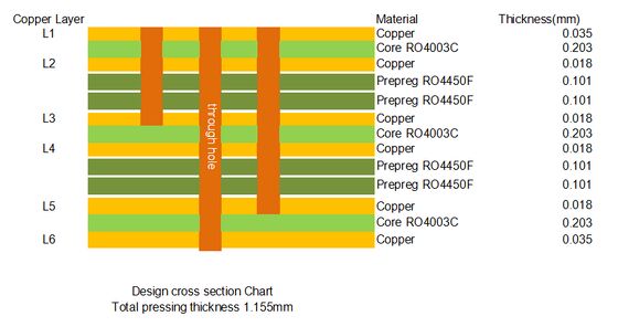
Deze printplaat is een 6-laags koperstructuur, en de materiaalsamenstelling omvat voornamelijk RO4003C kern, RO4450F prepreg en koperfolie.
Details printplaat
| Specificatie Item |
Details |
| Laagstructuur |
Bovenste laag (0,203 mm RO4003C) + 2 STUKS RO4450F Prepreg + Middelste laag (0,203 mm RO4003C) + 2 STUKS RO4450F Prepreg + Onderste laag (0,203 mm RO4003C) |
| Koperdikte |
Buitenste laag (L1, L6) - 1oz afgewerkt koper (0,035 mm); Binnenste laag (L2-L5) - 0,5oz afgewerkt koper (0,018 mm) |
| Gepersde dikte |
1,155 mm |
| Oppervlaktebehandeling |
Bovenste en onderste lagen met groene soldeermasker en witte zeefdruk; Onderdompeling goud |
| Afmeting |
92,5 mm × 77,3 mm (1 STUKS) |
| Speciaal proces |
Back drilling (L1-L3, L1-L5) |
Printplaat Stack-up
| Laag nr. |
Beschrijving |
Dikte |
| 1 |
Koperlaag — L1 (Buitenste boven, 1oz afgewerkt koper) |
0,035 mm |
| 2 |
Kern RO4003C |
0,203 mm |
| 3 |
Koperlaag — L2 (Binnenlaag, 0,5oz afgewerkt koper) |
0,018 mm |
| 4 |
Prepreg RO4450F |
0,101 mm |
| 5 |
Prepreg RO4450F |
0,101 mm |
| 6 |
Koperlaag — L3 (Binnenlaag, 0,5oz afgewerkt koper) |
0,018 mm |
| 7 |
Kern RO4003C |
0,203 mm |
| 8 |
Koperlaag — L4 (Binnenlaag, 0,5oz afgewerkt koper) |
0,018 mm |
| 9 |
Prepreg RO4450F |
0,101 mm |
| 10 |
Prepreg RO4450F |
0,101 mm |
| 11 |
Koperlaag — L5 (Binnenlaag, 0,5oz afgewerkt koper) |
0,018 mm |
| 12 |
Kern RO4003C |
0,203 mm |
| 13 |
Koperlaag — L6 (Buitenste onder, 1oz afgewerkt koper) |
0,035 mm |
| Totale gepersde dikte |
1,155 mm |

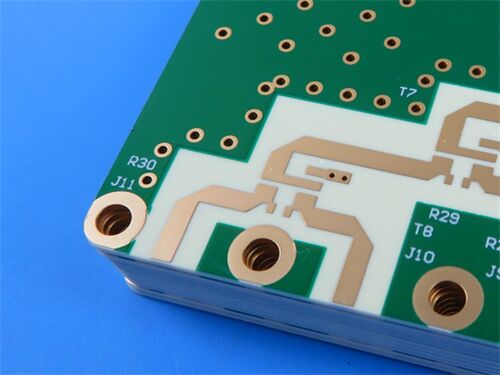
Wat is Back Drill?
Back drill (Back Drilling) is een speciaal boorproces dat wordt gebruikt bij de productie van high-speed en high-frequency printplaten, waarvan het kerndoel is om het niet-geleidende overtollige koperen pilaar deel (genaamd "stub") in het via-gat te verwijderen, om zo de integriteit van de signaaloverdracht aanzienlijk te verbeteren.
In meerlaagse printplaten gebruiken signaallijnen die verschillende lagen verbinden meestal via's, die doorgaans de volledige dikte van de printplaat doordringen. Wanneer een signaal van de ene laag (zoals Laag 1) naar de doel-laag (zoals Laag 3 of Laag 5) wordt verzonden via een via, heeft het deel van de via onder de doel-laag (uitlopend naar de lagere lagen) geen elektrische verbindingsfunctie, en deze overtollige koperen pilaar is de "stub". Bij hoge snelheden of hoge frequenties gedraagt de stub zich als een korte antenne, wat ernstige signaalreflectie veroorzaakt, leidend tot signaalvervorming, timingverschuiving, sluiting van het oogdiagram, en zelfs systeemfoutcodes of storingen.
Het back drilling proces lost dit probleem op door middel van secundair boren: na voltooiing van het conventionele printplaatproductieproces wordt een boor met een diameter die iets groter is dan het oorspronkelijke via-gat gebruikt om vanaf de achterkant of zijkant van de printplaat te boren, en de boordiepte wordt nauwkeurig gecontroleerd om precies door het deel onder de doel-laag te boren, om zo de stub fysiek te verwijderen. Na verwijdering is de resterende gatwand een niet-geleidend substraat dat niet langer deelneemt aan signaaloverdracht, wat signaalreflectie en -verlies aanzienlijk kan verminderen, de signaaloverdrachtssnelheid kan verbeteren, jitter kan verminderen en de signaalkwaliteit kan optimaliseren. Vergeleken met andere oplossingen zoals HDI blind/buried via's, is back drilling kosteneffectiever voor scenario's die high-speed via's vereisen, maar geen extreem hoge lagen.
In dit printplaatgeval wordt back drilling toegepast op de bereiken van L1-L3 en L1-L5, wat de signaalintegriteit van high-speed transmissie in de printplaat effectief kan waarborgen.
Introductie tot RO4003C
RO4003C is een eigen, met glasdoek versterkt, keramisch gevuld koolwaterstof composietmateriaal ontwikkeld door Rogers Corporation, dat de uitstekende elektrische prestaties van PTFE/glasdoek combineert met de verwerkbaarheid van epoxyhars/glasdoek. Het materiaal heeft twee verschillende configuraties met 1080 en 1674 glasdoeken, en alle configuraties hebben dezelfde elektrische prestatiespecificaties. Het heeft strikte procescontrole, stabiele en consistente diëlektrische constante (Dk) en lage verlieskenmerken, en zijn unieke mechanische eigenschappen maken het gelijk aan het standaard epoxyhars/glas verwerkingsproces, terwijl de kosten veel lager zijn dan die van traditionele microgolf laminaten. In tegenstelling tot PTFE microgolfmaterialen vereist dit materiaal geen speciale via-verwerking of bedieningsprocedures.
Belangrijkste parameters van RO4003C (Kerninhoud van datasheet)
| Parameter |
Typische waarde |
Opmerkingen/Testmethode |
| Diëlektrische constante (Dk) @10GHz |
3,38 ± 0,05 |
Typische proceswaarde; Typische ontwerpwaarde is 3,55 |
| Verliesfactor (Df) @10GHz |
0,0027 |
Typische waarde, met uitstekende low-loss prestaties |
| Z-as thermische uitzettingscoëfficiënt (CTE) |
46 ppm/°C |
Typische waarde, -55°C tot 288°C |
| Volume weerstand |
1,7×10¹⁰ MΩ•cm |
Typische waarde, goede isolatieprestaties |
| Waterabsorptie (D48/50%) |
0,04% |
Typische waarde, uitstekende vochtbestendigheid |
| Thermische geleidbaarheid @50°C |
0,71 W/m•°K |
ASTM D5470, goede warmteafvoer prestaties |
| Peel Strength (1oz ED Foil) |
6,0 lb/inch (1,05 N/mm) |
Typische waarde, sterke bindingskracht met koperfolie |
| Vlamvertragende klasse |
Niet FR |
Voldoet niet aan UL 94 V-0 standaard |
| Compatibiliteit met loodvrije processen |
Ja |
Geschikt voor loodvrije assemblageprocessen |
Toepassingsgebieden van RO4003C
Dankzij zijn uitstekende elektrische prestaties, verwerkbaarheid en kosteneffectiviteit wordt RO4003C veel gebruikt in microgolf-, high-frequency en high-speed elektronische apparatuur, voornamelijk inclusief:
Communicatie-infrastructuur: Mobiele basisstationantennes, radio backhaul apparatuur, telecommunicatie-grade Wi-Fi/geautoriseerde hulp toegangssystemen, IP-infrastructuur en point-to-point microgolf communicatieapparatuur.
Automotive Intelligentie: Automotive radarsystemen en sensoren, ter ondersteuning van de ontwikkeling van autonome rij- en voertuigveiligheidstechnologieën.
High-frequency en High-speed apparatuur: Phased array radarsystemen, eindversterkers, high-speed servers (CPU/GPU/geheugen interconnectie), high-speed netwerkcommunicatieapparatuur (routers, switches, optische modules).
Internet of Things (IoT): RFID-antennes, ter verbetering van de identificatienauwkeurigheid en signaaldekking.
Andere gebieden: Test- en meetapparatuur, lucht- en ruimtevaart- en defensie-elektronicasystemen, en andere apparatuur die Gbps-niveau high-speed digitale signalen of radiofrequentie microgolfsignalen moet verwerken.

 Uw bericht moet tussen de 20-3.000 tekens bevatten!
 Dutch
Dutch